Semiconductors are censorious for electronics manufacturing companies development. A faithful source of semiconductors is thus strategic to correct information structure and allow digital metamorphosis. This has been powered by elaboration of Artificial Intelligence technology and emergence of substance of operations in the society and frugality. This blog deals the use cases of AI in design and manufacture of semiconductors and transferring semiconductors request by applying AI technology workloads in important sectors of frugality.
Semiconductor
assiduity is traditionally and notoriously known to be largely capital and
technology ferocious.
This
is in favor of complicated and expensive ministry involved in manufacture, need
for access to serviceability similar as clean and plenitude of water and
continued clean electric power and actuality of effective force- chain from
product bottom to consumer. The other reason is largely professed force
involved in designing special purpose semiconductor chips which is precious to
hire. Coupled with this are high pitfalls due to rapid-fire changes in
technology, long gravidity period for products to face and accordingly long
vengeance ages. This is the main reason why there are only a many successful
companies the world over across a many countries that are enwrapping a
leadership position as a global supplier of semiconductor fabrication factors
of different types.
Table below gives an idea of capital and design costs involved in a semiconductor design and product eco system, as per the numbers reported by Mc Kinsey.

This is pushing the semiconductor
companies to lifelessly work through innovative processes to minimize chip
product processing times and increase productivity using technology inputs in
both design and fabrication.
In a traditional technology mound the
semiconductors needed are for storehouse, memory, sense and networking. Among
these, while the processors continue to enthrall the premier position chasing
the Moore’s law by shrinking the line extents to 5 nanometers, as per an IRDS
report, storehouse will witness the loftiest growth due to humongous quantum of
data that's stored and is needed to be reused for inferring intelligence in the
operation concerned. But the semiconductor assiduity will continue to reap
utmost gains in computing, memory and networking results creating stylish
occasion for value creation.
No country is 100 independent in their semiconductor conditions indeed as the countries specially leading the force are Taiwan, South Korea, Japan, USA and China. Following table gives the chance share of semiconductor foundries profit encyclopedically, and the semiconductor assiduity global request share country wise, and shows how lob sided the spread is as follows;

Still, these veritably
countries are seeking heavy investments in design and manufacturing of
semiconductors to capture a larger share of global request and maintain a
leadership position performing in accelerated profitable growth and giving a
strategic advantage to the country encyclopedically.
India presently imports its 100 of
semiconductor conditions with an estimated significances of products worth US$
15 billion in the time 2020, as per sources from MeitY. The irony is that India
enjoys the distinct status of a leading global semiconductor chip developer
with roughly 20,000 masterminds engaged in this profession working for
virtually all major global semiconductor manufacturers. We'll deal with this
latterly in this paper.
therefore far, PCs and Mobiles have been the
largest consumer of semiconductors due to their exponential growth in the
former decade. With demand in these sectors the semiconductor assiduity has to
review its strategy to concentrate on other sectors that promise potentially
high request growth to sustain return on investment. As per the data released
by IRDS, the semiconductor assiduity is only suitable to capture 20- 30 of the
total value of PC mound and simply 10- 20 of the smart phone request. Such a
diminished value creation isn't enough to justify the capital investment made
in design and manufacturing of semiconductor bias unless it brings in invention
to find newer openings and request part.
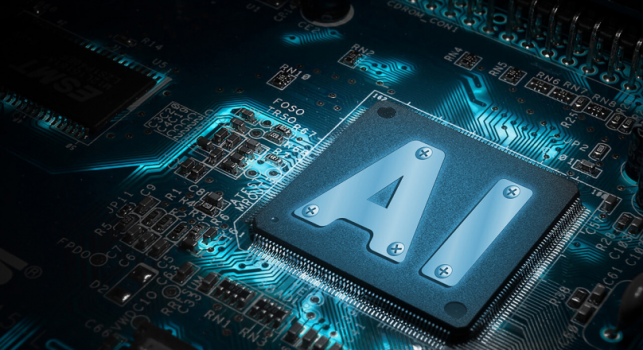
“The revolution in Artificial Intelligence technology and its implicit operations comes as a deliverance to the semiconductor assiduity furnishing it the topmost occasion in the current time to produce value of the kind it has had in the former decades.”
Semiconductor
Industry reconsidering its Strategy
With
the requests for semiconductors drenching in the heretofore fast- moving
sectors of PCs and Mobiles, and significant investments formerly having been
made by the assiduity, the semiconductor assiduity has formerly readdressed its
strategy to work with the areas that won't only continue to return on the
investments formerly made but also justify newer investments in custom designs
and manufacture. The focus is now shifting on independent vehicles, artificial
robots, IoTs, drones etc, numerous of which are driven by the conception of
Assiduity4.0.
The operations being viewed with interest then
are for semiconductors demanded in bedded AI for facial recognition, speech-
to- textbook, particular adjunct, navigation and hunt, and use of AI
technologies in high- performance computing for complex simulation & modeling,
determining data patterns and vaticination, data analytics and decision support
functions.
At the core of this new strategy lies the technology
of artificial intelligence( AI).
The
colorful arising AI operations partake a one common point- that's reliance on
tackle as a core enabler of invention, especially for cipher and memory
functions. The strategy thus embeds into it a binary part of AI towards new
semiconductor conditions, as explained below.
One is applying AI/ ML use cases to
semiconductor manufacturing and designs to optimize on costs. As the
manufacture of semiconductors is the largest cost motorist, as per a McKinsey
estimate, AI/ ML will accrue utmost value- upto about 40- and drop in costs by
about 17 through robotization and verification during product cycles, effective
tool design for enhanced performance, use of computer vision for examination,
assess tool fatigue, help machine down times and minimize overall chip product
processing time. Further, for semiconductor design apply AI/ ML use cases to
avoid time consuming duplications and ramp up yield to reduce costs conceivably
by over to 28- 32%